
Semiconductors
Credit: The Schools' Observatory
Semiconductors are an important part of CCD cameras (Charge-coupled Devices). They help to convert light into a current in the technology. Unlike conductors such as metals, semiconductors are not able to conduct current. This is because they have no free electrons. The most common material used in semiconductors is silicon which only conducts electricity under certain conditions.
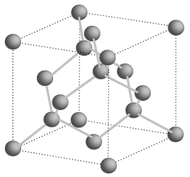
Silicon atoms can be stacked to make a crystal. These have regular structures with atoms bound by sharing a pair of electrons. A silicon crystal can't conduct current because the electrons are not free. To change this a small amount of energy can be put into the system. This frees the electrons.
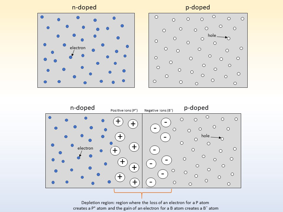
It is possible to make semiconductors better using a process called doping. There are 2 different types of doping. In both cases a different material is added to the crystal. The 2 types are called n-doping and p-doping:
n-doping: Here silicon is doped with a material like phosphorus (P). This replaces some silicon atoms in the crystal. The silicon bonds with the phosphorus but leaves behind an extra electron. This is loose inside the crystal and can be freed easily. This lets it conduct electricity. The electrons that are freed have a negative charge, so the process is called n-doping.
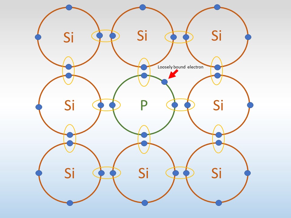
Image of silicon (Si) atoms bonding to phosphorus (P) inside a crystal. The P atom has a spare electron which is loosely bound.
Note: The rings only show the electrons in the outer shells of the atoms.
Credit: The Schools' Observatory
p-doping: Here the silicon is doped with an atom like boron (B). Like n-doping, the silicon wants to bond four silicon atoms. But boron only has 3 electrons available. The extra electron comes from a neighbour atom. This makes a hole in the parent atom's outer shell. Once this hole is opened, another electron moves to take its place. The hole moves around the crystal! With a positive charge this is called p-doping.
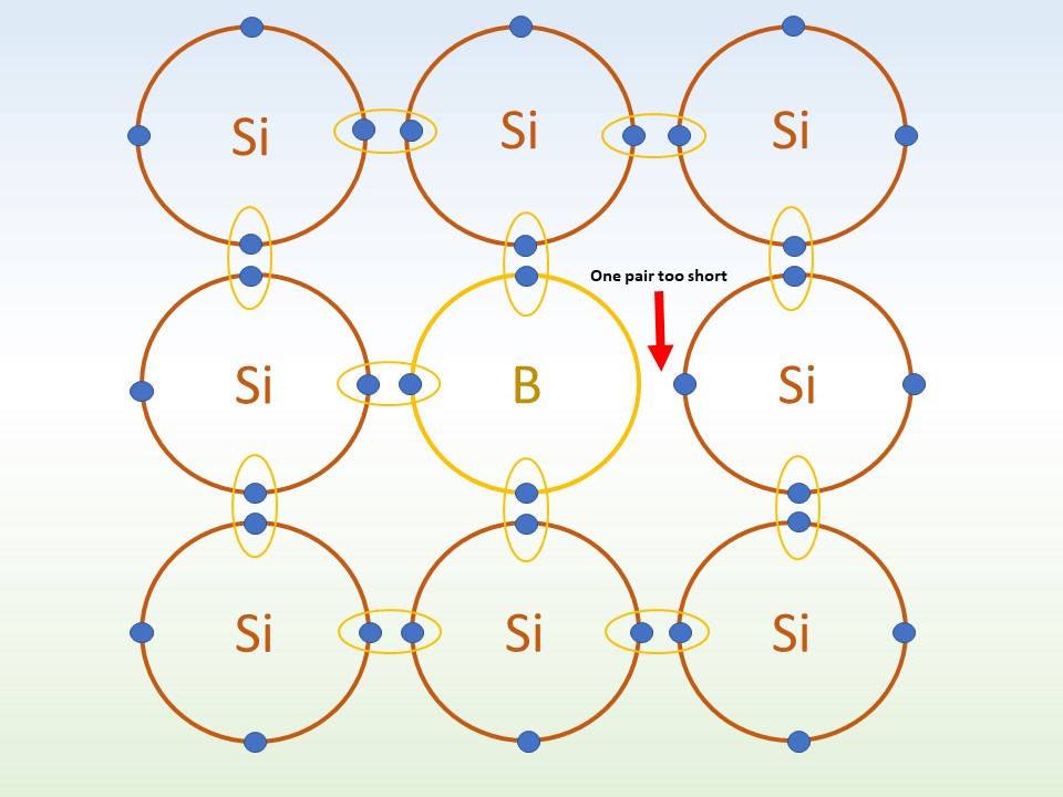
1. The 3 electrons in the outer shell of the B atom form bonds with 3 Si atoms, but there is one bond left.
Credit: The Schools' Observatory
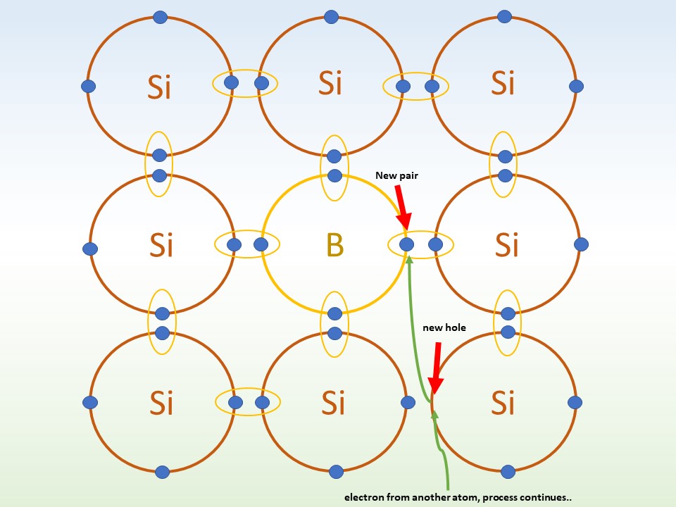
2. An electron from another atom jumps to fill the hole, but once this hole is filled another takes its place.
The hole moves through the crystal.
Credit: The Schools' Observatory
To get a conductor we then need to join an n-doped and p-doped material together.
When an n-doped and p-doped material are joined together they make a diode. The free electrons in the n-doped material will move across to fill the holes in the p-doped material. The holes in the p-doped material will also move across to join with the free electrons! This switches the charge of the n-doped region to positive and the p-doped region to negative. This makes an electric field across the join between the 2 materials. The small area around this join is called the depletion region. This stops any more electrons moving across unless some energy is applied.
the holes move to join with the electrons in the n-doped region.
Credit: The Schools' Observatory
How does this work in a CCD chip?
CCD chips are made from doped silicon materials. They convert photons of light to charge using the Photoelectric Effect.
When a photon hits the loose electrons in the n-doped material, it gets energy. We call this a photoelectron. The energy is enough for the electron to become free. If there are a lot of photons then these make a lot of free electrons. These have enough energy to move across the depletion region and make an electrical current.
There is a limit to how much charge can be stored in this depletion region. Pixels will not saturate as easily if they can collect more charge before 'overfilling'. To do this more doping is added to the silicon. This can’t be done forever. Too much doping can increase the noise in the chip, something called dark current. This makes the data harder to read.